Welcome to the Lightwave Research Laboratory!
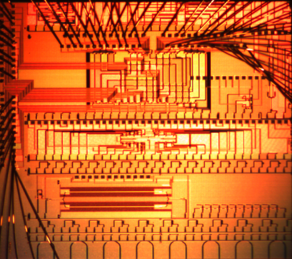
The Lightwave Research Laboratory is involved with multiple research programs on optical interconnection networks for advanced computing systems, data centers, optical packet-switched routers, and nanophotonic networks-on-chip for chip multiprocessors. We are developing a new class of nanoscale photonic interconnect technologies that seamlessly move data from on-chip networks, across memory and large computing systems with extreme energy efficiency. These future platforms, driven by nanophotonic-enabled interconnectivity, and the enormous bandwidth advantage of dense wavelength division multiplexing, will fundamentally transform the computation-communications architecture, to create systems able to meet explosive information demands at all scales.
With the growing demand for photonics based technologies in data centers and high performance computing applications, the Lightwave Research Laboratory aims to be on the cutting edge of research while creating feasible and deployable solutions to tackle real challenges faced in industry.
Join Us!
We currently have openings for Postdoctoral Fellows, PhD candidates, and MS students in our group! Interested candidates should contact Professor Bergman at [email protected] with their resume/CV and cover letter. We look forward to hearing from you!
Recent Publications
-
Ultra-Efficient Foundry-Fabricated Resonant Modulators with Thermal Undercut
-
Efficient Silicon Photonic Add-Drop Microdisk Filters for DWDM Systems
-
Integrated, Compact, and Tunable Band-Interleaving of a Kerr Comb Source
-
Universal CMOS-Foundry Compatible Platform for Ultra-Low Loss SOI Waveguide Bends
-
Ultra-dense 3D integrated 5.3 Tb/s/mm2 80 micro-disk modulator transmitter
-
CMOS-Foundry Compatible, Broadband, and Compact Routing of Multimode SOI Waveguides
-
Simultaneous Error-Free Data Modulation with Silicon Microdisks in the Multi-FSR Regime for Scalable DWDM Links
-
SiP Architecture For Accelerating Collective Communication in Distributed Deep Learning
-
Low-Loss Wide-FSR Miniaturized Racetrack Style Microring Filters for ⩾1 Tbps DWDM
-
Dispersion-Engineered and Fabrication-Robust SOI Waveguides for Ultra-Broadband DWDM
-
Scalable architecture for sub-pJ/b multi-Tbps comb-driven DWDM silicon photonic transceiver
-
Process Variation-Aware Compact Model of Strip Waveguides for Photonic Circuit Simulation
-
Fabrication-robust silicon photonic devices in standard sub-micron silicon-on-insulator processes
-
Petabit-Scale Silicon Photonic Interconnects with Integrated Kerr Frequency Combs
Recent News
Professor Bergman Presents at the 2023 DARPA ERI Summit
Professor Bergman presented "Challenges and Solutions to DATA I/O" at the 2023 DARPA Electronics Resurgence Initiative (ERI) Summit.
Professor Bergman Hosts Inaugural CUbiC Conference at Columbia
At the inaugural annual review of Columbia Engineering’s Center for Ubiquitous Connectivity (CUbiC), held June 27-28, faculty, students, researchers, industry experts, and government officials convened to discuss new and ongoing research and share insights, fostering collaboration and driving advancements in the field of ubiquitous connectivity. Attended by about 115 in-person guests and additional participants who joined virtually, the two-day event at Columbia’s Morningside campus delved into three research themes: connectivity networks and systems, wireline and lightwave interconnects, and wireless circuits and technology.
Transferring Data with Many Colors of Light Simultaneously
Our recent Nature Photonics publication, "Massively scalable Kerr comb-driven silicon photonic link" was highlighted in an article by Columbia Engineering. This work demonstrated chip-scale wavelength-division multiplexing, with 32 channels operating at 16 Gbps, achieved via a Kerr comb source designed by our collaborators in the Lipson and Gaeta groups.
Paper Featured on the Front Cover of IEEE Journal of Selected Topics in Quantum Electronics

We need a rethinking of the boundaries between communication and computation and to fundamentally reinvent how data moves across systems with minimal energy consumption.