Past Projects
Rockport Networks Inc. provides software solutions for enterprise data center networks in Canada and the United States. They are working on an autonomous networking model that reduces data center power consumption and improves network performance by employing optical switches. Rockport Networks Inc. sponsored a research project with LRL to investigate: 1. Novel photonic switch architecture designs for low-radix switch circuits using physical layer simulation tools. 2) Evaluation of integrated silicon switch fabrics. 3) Enhancement of simulation infrastructure to evaluate the scalability of data center networks and data center traffic patterns.
Engineering Research Center (ERC): Center for Integrated Access Networks (CIAN)
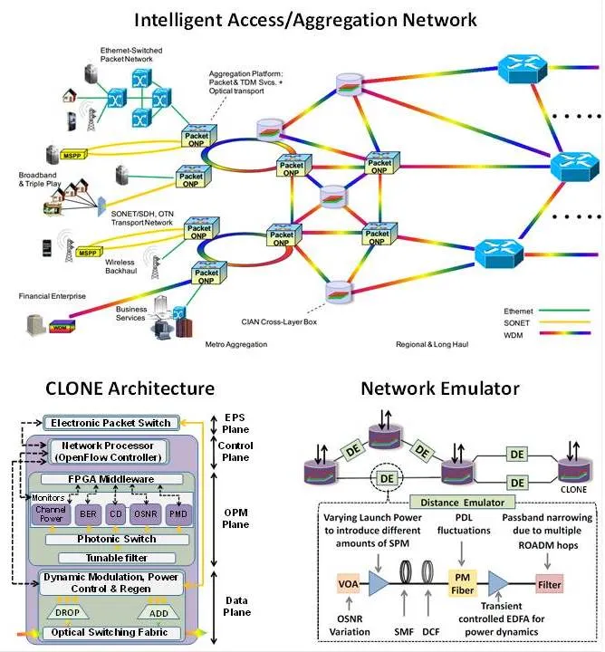
Ever-growing demand for speed and bandwidth and increasing energy consumption in today's networks are driving the need for intelligent next-generation networking architectures that can overcome fundamental spectral and energy limitations. CIAN, an NSF-funded engineering research center is a multi-university consortium that aims to overcome the bottle-necks the existing static, tiered aggregation network by transforming it into a dynamic, on-demand service-aware network. Our role, as the CIAN networking thrust lead, is to develop this envisioned intelligent access/aggregation network that will seamlessly interface with the edge/core and dynamically deliver most demanding high-bandwidth applications at low-cost and extreme energy efficiency.
One of the key building blocks of our intelligent access/aggregation network is a hybrid electronic and optical switching node that we have designated as the cross-layer enabled optical network element (CLONE). The CLONE provides real-time introspective access to the optical layer in conjunction with awareness of higher layer network constraints (e.g., application, quality of service requirements, and energy consumption) to make more informed routing, regeneration, modulation, and power control decisions. This intelligent interaction between the network layers will result in improved network performance and enable scalable aggregation of heterogeneous service traffic. Another major effort is the network emulation test-bed which is used to replicate the transmission impairments and dynamics for networks of variable size and topology. This test-bed allows us to stringently study any system of interest under real network conditions, enabling us to evaluate and validate the performance of the evolving CIAN box and other novel photonic technologies.
Dynamic Optical Networking
Dynamic optical networking, where bandwidth is allocated on-demand in the physical layer in response to changing traffic demands and network conditions, is a promising solution to address the energy and capacity challenges in the current network. However, rapidly reconfiguring light-path connections causes unpredictable transmission impairments and result in network instability.
Physical Layer Techniques
To achieve dynamic networking capabilities, it is first necessary to fully understand the additional network instability and uncertainty that will be caused by dynamic operation so that compensatory methods can be developed. We use the network emulation test-bed to study and characterize the transmission impairments and dynamics that affect WDM circuit switching and all optical aggregation networks. Since the impairments under dynamic operating conditions are unpredictable, the optical layer has to be monitored real-time so that the appropriate compensatory techniques can be rapidly executed. Ubiquitous deployment of monitoring devices is thus key to achieving a dynamic optical network. However, this will be a feasible solution only if the monitoring devices and cost-effective, energy efficient and supports multiple data formats. We are focused on developing fast monitoring solutions for advanced data formats and enabling these devices to function autonomously. We are also investigating methods of re-configuring light-paths such that accompanying dynamics do not cause data loss.
Algorithms
Our collaborator, Dr. Gil Zussman, has developed cross-layer network control algorithms to stabilize optical signals in rapid light-path reconfiguration scenarios. These algorithms builds on the capabilities of new devices and will allow efficient use of optical resources through dynamic network configuration, and physical layer power, bandwidth, and modulation control. The algorithms are used in the network emulation test-bed along with new monitoring devices to investigate the time to converge to a stable operating point in dynamic networks of various size, topology and complexity.
Optical Accelerators for Data Center Networks
Optical accelerators are passive and active optical modules or sub-systems that provide fast and efficient data transmission for certain applications. The main challenges in implementing the end-to-end system containing optical modules are the integration with current Ethernet-based networks and the control and configuration of them. Software Defined Networking (SDN) along with cross-layer designs can overcome these challenges and provide optical accelerators seamlessly to the higher layers.
We have presented multicast traffic acceleration for intra data center networks using passive optical splitters. Our design is compatible with hybrid networks and its implementation requires only commodity optical components. Optical accelerators reduce switching energy consumption and latency comparing to transmission over electrical packet switching network.
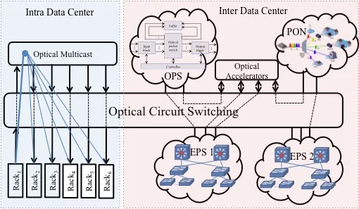
Converged Inter/Intra Data Center Network
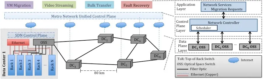
The rapid growth in cloud-based services and video streaming is changing the traffic size and pattern in the optical transport networks. According to the studies, by 2017, the metro traffic increases by 560% and 75% of the overall traffic will be terminated within the metro network. Regional data centers are the significant contributors to this traffic. Companies employ mid-size data centers in the metro distances that actively communicate for the services such as virtual machine (VM) migration, backup, video streaming, load balancing or fault/disaster recovery. This growth and shift in the metro traffic characteristics necessitates flexible designs with fast reconfiguration and seamless communication within network layers.
We have designed a novel converged inter/intra data center architecture in metro-scale distances using commodity optical space switches (OSS). We employ OSS to route both east-west and north-south traffic by aggregating racks inside the data center and also providing uplink for inter data center connectivity. The network management in the metro region is through a unified SDN control plane. A 3-layered architecture is designed to receive and schedule service requests from the application layer, and configure optical nodes in the physical layer. We have experimentally demonstrated live migration of VMs among 3 data centers over 50 km. Our design provides seamless connectivity between the application and physical layers and faster network reconfiguration in metro regions.
Due to the accelerated growth in performance of microprocessors and the recent emergence of chip multiprocessors (CMP), the critical performance bottleneck of high-performance computing systems has shifted from the processors to the communications infrastructure. By uniquely exploiting the parallelism and capacity of wavelength division multiplexing (WDM), optical interconnects offer a high-bandwidth, low-latency solution that can address the bandwidth scalability challenges of future computing systems.
High-Performance Computing and Memory Interconnects Using Silicon Photonics
The limitations of main memory accesses have become a bottleneck for the scaling of high-performance computing systems. Memory systems must balance requirements for large memory capacity, low access latency, high bandwidth, and low power. As such, the electronic interconnect between a processor and memory is a key consideration in overall system design. The current trend in memory system design is to access many memory devices in parallel and transmit data over a high-speed, path-length-matched, wide electronic bus. Overall, the increasing number of memory devices, higher bus data rates, and wiring constraints are pushing the limits of electronic interconnects and threatening the performance gains of future computing systems. Optically-connected memory systems can enable continued performance scaling through high-bandwidth capacity, energy-efficient bit-rate transparency, and time-of-flight latency. Memory device parallelism and total capacity can scale to match future high-performance computing requirements without sacrificing data-movement efficiency.
Our optically-connected memory system provides an all-optical link between processing cores and main memory across an optical interconnection network, such as the interconnect fabric system test-bed. By implementing the processing cores on FPGAs we can explore novel memory architectures and model various applications. We have the ability to perform in-depth architectural exploration and validation, and we are working to close the growing performance gap between processors and memory.
Only a portion of the processor-to-memory performance gap can be answered by simply inserting conventional telecommunications-grade optical components in current computing hierarchies. The silicon photonics platform promises to bring low-cost, low-energy, and small footprint optical interconnects to the forefront, resulting in tight integration between computational components and optical interconnects. Effective silicon photonic modulators, filters, and switches have been demonstrated at the device level for high-bandwidth and dynamic functionality; however, such devices lack unified and well-developed integration. By integrating control plane logic with device-level functionalities such as wavelength division multiplexing (WDM), wavelength routing, and broadband spatial switching, we can provide a set of optical network primitives and a new paradigm for delivering computational data and processor-to-memory transactions.
We are further investigating FPGA-enabled silicon photonic interconnects for computational and processor-to-memory interconnects, expanding on our work with OCM architectures. We have developed an FPGA-based optical network interface that can execute primitives compatible with OCM data transactions. In investigating such functionalities, we can demonstrate network transaction paradigms of OCM interconnections, paving the way for new silicon photonics enabled computing systems.
Photonic Networks for Hardware Accelerators in Utility Computing
All the the industry's biggest tech players are chasing the cloud-computing market these days, and for good reason, cloud computing is poised to a huge rewards field in the next few years. In other words, the paradigm shift from buying a single CPU computer to renting them has begun. This repackaging of computing services, known as utility computing, has become the foundation for the shift to "on demand" computing, sofware and gaming as a service and cloud computing models that continue propogating the idea of computing, applications, and network as a service. Heterogeous computing within these systems - the use of different hardware acclerators (x86 CPUs, FPGAs, GPUs) to coorperate on one computing task- is quickly on the rise. Current architectures however only allow for localized hardware accleration.
High-bandwidth connectivity provided by Wavelength Division Multiplexing (WDM) optical interconnects is an important enabler for delocalized hardware accelerators in heterogeneous utility computing. In this work, we build a testbed for optically connected hardware accelerator emulatiors on an FPGA-based system. We have the ability to perform in-depth architectural exploration and validation of the functionality and advantages of an optically connected heterogeous utility computing system.
Optical Network Interface and Protocol Development
While small-scale integrated silicon photonic devices have been demonstrated in recent years with high-bandwidth and energy-efficient performances, the benefits at the system level are yet to be realized. A systems-level implementation that aims to extract performance gains on real applications requires a completely programmable interconnection network. Maximal optical network utilization can be achieved by intelligently arbitrating wavelength routing and spatial circuit switching, which are key functionalities of silicon photonic architectures. A programmable interface must therefore implement all the required network protocols in such a way that they are compatible with protocols specific to operating silicon photonic devices. With programming methodologies available for silicon photonics devices that adhere to optimal network behaviors, these emerging devices can be architected to function and deliver their aforementioned performance benefits at the system level in a fashion that is fully integrated with system software.
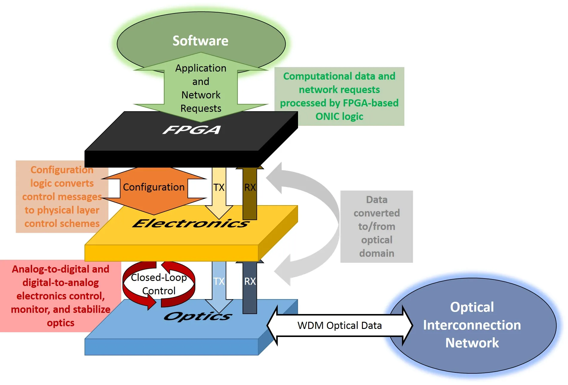
Such tightly integrated hardware-software design is facilitated by our FPGA-based optical network interface (ONIC) logic. Historically, the "C" in ONIC stands for "card", but in recent work is deprecated as the ONIC has been expanded to operate on many different custom and commercial-off-the-shelf FPGA mainboards. Our ONIC employs logic to control wavelength stabilization and routing (with available digital-to-analog and analog-to-digital circuitry and closed-loop control), patterned data validation (PRBS and BERT) for established optical links via standard SerDes/electrical transceivers, and data delivery mechanisms coupled to JTAG- and Ethernet-connected software coprocessors. Our silicon photonic interconnection network testing and validation platform employs multiple FPGAs and ONICs for validation and verification of control-, network-, and application-dependent protocols. Application execution on our FPGA-enabled ONIC propagates from hardware-software co-implemented instruction-set architectures to an out-of-band control message passing interface that establishes different configurations among many interconnected FPGA-controlled silicon photonic devices in a best-effort, semi-simultaneous way.
Such a system allows for system-level validation and implementation of custom applications that can take advantage of optics-enabled network primitives. In this regard, application kernels cannot necessarily execute in an optimal way on an arbitrary optical interconnection network, so new methodologies must be developed to include optical network behaviors at the kernel and perhaps even instruction level.
Silicon photonics (SiP) is emerging as a leading candidate for addressing the power and bandwidth challenges of next generation on- and off-chip interconnects due to its compatibility with complementary-metal-oxide-semiconductor (CMOS) process, ultra-small device footprint, low power consumption and high bandwidth. Small footprint allows fitting hundreds to thousands of these devices on a single chip, thus allowing true scalability of the i/o bandwidth. As the power consumption is proportional to the device volume (through the amount of electrical carriers that need be injected), the power consumption of such devices, at 10 fJ/bit, is also orders of magnitudes smaller than other structures. Hypothetically, this in turn enables < 1 pJ/bit link power efficiencies.
Silicon Photonic Devices for High Throughput Transmission Links
A significant part of our research is devoted to investigating the characteristics of various nano-photonic devices for application in telecom and datacom systems. All components necessary for a transmission link have been demonstrated and characterized including transceivers, modulators, filters and receivers. Ongoing research efforts are directed towards realizing dense WDM, various modulation formats for increased laser power utilization and further improving and optimizing device characteristics in collaboration with device design groups.
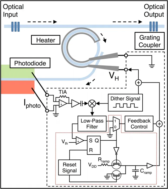
Thermal stabilization and initialization of microring devices
Microring devices have the advantage of small-footprint, energy efficient operation, and intrinsic WDM compatibility. They are especially promising for use in the CMOS-compatible silicon photonics platform to replace electrical interconnects in next generation datacenters and supercomputers. One challenge facing commercial usage of microrings is their thermal sensitivity. Because of the high thermal optic coefficient of silicon the resonance location of microrings shift around 0.8 nm/K. Our group has pioneered active thermal feedback systems based on dithering, where a small periodic signal applied to the heater is used to derive the location of the microring resonance. The dither technique overcomes the symmetry of the microring resonance and allows simple feedback circuitry to be used. This technique has been applied to thermally stabilize multiple microrings at the same time for WDM operation.
Fast thermal initialization of microring devices is also possible by leveraging the dithering method. Due to fabrication variation, the initial resonance location of a microring will be slightly different from the intended operating laser wavelength in the system. Thus an initialization sequence is necessary to lock the microrings to the lasers. We demonstrated that the initialization process can be accomplished within an order of magnitude of the thermal time constant of the microring system.
Silicon Photonic Switches
High-port-count optical space switches, long of interest in long-haul systems, have found renewed interest in data centers to provide high bandwidth connections on demand. We have demonstrated the applicability of SiP Mach-Zehnder and microring based device for optical switching and we continue to study their scalability.
In our endeavor to investigate practical microring resonator-based dynamic switching functionalities within this silicon platform, we have characterized a multi-wavelength 1×2 switch, capable of switching optical signals with data rates approaching terabits-per-second. Subsequently, we examined a 2×2 switch, which also enables dynamic message routing of wavelength-parallel broadband photonic signals. Combining the demonstrated 1×2 and 2×2 switching functionalities, we then investigated a thermally active 4×4 switch, which enables non-blocking switching functionality within complex network architectures.
In addition to the design and implementation of these components, we have characterized their predominant signal-degrading impairments in an effort to further improve the performance of interconnection networks derived from future versions of these devices. Narrowband filtering of high-speed data signals is an important consideration when passing data through high-quality-factor microring resonators, as is done in the aforementioned multi-wavelength switches. We have experimentally and numerically characterized the power penalty induced by this effect, and applied the numerical simulator to a wide variety of other higher order transfer functions realizable with these devices.
Advances in multicore architectures have produced increased parallelism in computation, and as a result data movement rather than raw computation has come to determine system performance in data centers and high performance computational systems. The fundamental limitation in increased data movement is energy consumption: for electronic links, power dissipation scales with data throughput. Optical data transfer over silicon photonics offers a promising alternative as wave division multiplexing allows for high bandwidths and the bit-rate transparency of photonic systems means power consumption does not scale with data throughput. While point-to-point optical data transfer is a fairly mature area, data-dependent traffic exhibits several aspects of dynamic path dependence in computational systems. Frequently path changes may occur, which requires a switching fabric to respond to these demands in real-time with reasonable network utilization. For a photonic switching fabric to be of practical use, it must be energy efficient, have short reconfiguration times, maintain optical signal quality, and be scalable to larger switching sizes.
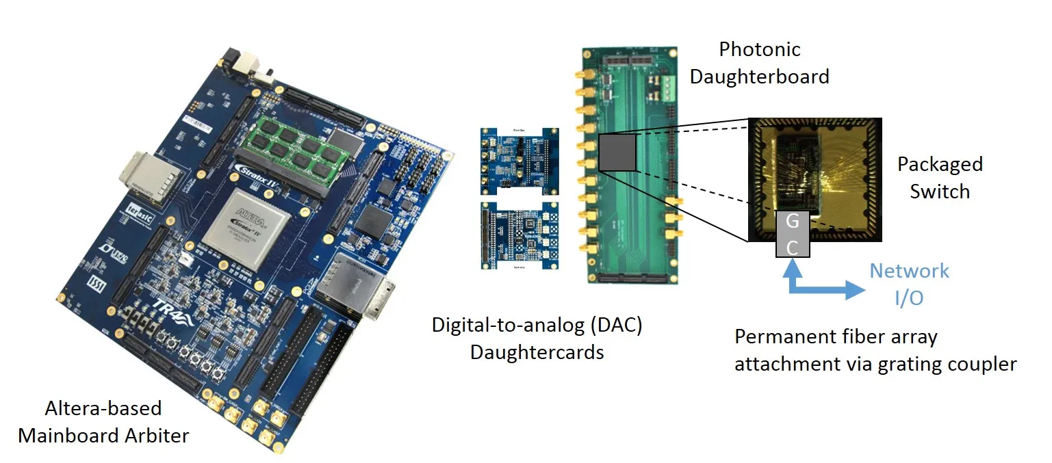
We are working towards developing and testing programmable switching fabrics composed of Mach Zehnder Interferometers (MZIs) and microring resonators. Single devices can act as 2x2 switching elements, whose switching behavior can be tuned with an applied voltage. Since volume devices are subject to manufacturing tolerances, device characterizations are necessary to accurately determine the applied voltages necessary for the appropriate behavior. By intelligently connecting multiple MZIs or microrings, larger switching fabrics can be constructed. We are using FPGAs as a central logic controller-dubbed the arbiter-connected to analog-to-digital and digital-to-analog electronics used to quickly actuate physical configurations of many photonic devices. Our arbitration system includes a higher control layer that is compatible with software and provides a control message passing interface.
A nanophotonic interconnection system, although equivalent to an electrical one on the principle (carriage and switching of information - while showing drastically improved performances), has its own peculiarities and design constraints. To create a new generation of photonic-enabled interconnection networks, the research effort must employ a co-design strategy that concurrently investigates computer and photonic-enabled network architecture designs. This re-assessment of the distributed computing architecture (i.e. from single Chip-Multiprocessor based systems to large scale, supercomputer typed systems) impacts in turn the application programming, which should be included in the co-design. Using our custom, in house designed simulations suite PhoenixSim 2.0, we, along with our collaborators model numerous multiprocessor architectures and networks.
Integrated Modeling Environment
A central component in our research effort is the development of an integrated modeling and design environment spanning multiple levels of abstraction from the physical level through the circuit and micro-architectural level up to the system level. Our targeted methodology has been presented in this paper .
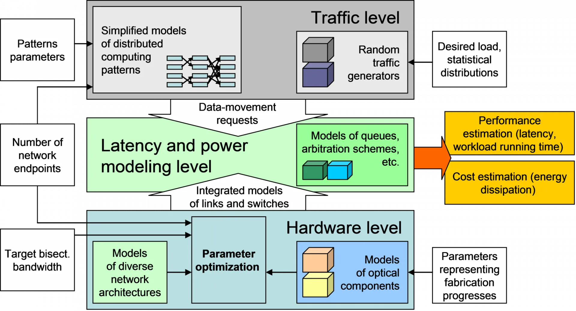
Our environment is called Phoenix Sim 2.0 and consists of three modules. The hardware level tool translates the characteristics of nanophotonic elements located along each link into insertion losses, power penalties and crosstalk metrics. This tool is based on models proposed in the literature but also on in-house developed ones. In particular, we recently we reported progresses on the modeling of integrated Silicon Photonics switch.
Starting from an initial architecture (bus, network), this tool is able to automatically assemble different designs, typically varying the scale, the nominal-per-wavelength datarate, and the number of wavelengths. Specific algorithms are used to identify the worst-case signal impairments under dynamic traffic. Each architecture is then analyzed and optimized to maximize throughput while maintaining signal integrity in any traffic condition.
Architectures developed and optimized with the physical layer can then be tested under dynamic traffic conditions using LightweightSim discrete-event simulator. A LightweightSim simulation can involve different type of traffic injectors. Using statistical traffic generators, the impact of the networking protocol and the associated contention resolution mechanisms present in the network can be statistically measured, which gives a rough estimate of the global system performance. In this case, LWSim translate the action taken at the micro-scale by the protocols and the devices into macro-scale statistical latency and bandwidth measurements. Check in particular this paper where we analyze different reservation protocols for an all-optical switch, and this study on the consequences in terms of energy of various reservation schemes.
LWSim also supports application dependent traffic. Specific injectors and receivers are created in the network simulation structure. In parallel, threads are created and associated with portions of code. Messages generated in that code are passed to the injectors, emitted in the network, received by the receivers and passed back to the threads. In this way, cross-influences between the executed code and the network can be analyzed.

The PhoenixSim 2.0 suite takes advantage of Javanco , a scientific computing toolbox. Javanco includes in particular versatile graph handling and visualization functionalities. Network layout displayed in above have been generated and displayed with it. Furthermore, LWSim simulations can be visualized live and network elements characteristics can also be modified through the graphical interface while the simulation is running. These features can be exploited to graphically check that a simulation model is correctly implemented, and that changes in the configuration change the performance as predicted. Javanco also integrates a graphical interface permitting an eased creation of simulation batches, which is extremely useful for design exploration. This semi-automated batch creation system is coupled with a result collection systems with integrated chart drawing functionalities.
Optically Interconnected Distributed Computing Systems
This effort aims to address the detrimental communications constraints imposed by bandwidth density limitations and vastly growing power consumption of current electronically interconnected systems. We aim to develop optical interconnection network architectures for rack to warehouse scale distributed computing systems. We leverage our modeling and simulation environment (PhoenixSim) to obtain energy-performance data movement analysis and optimize the systems for diverse workloads types.
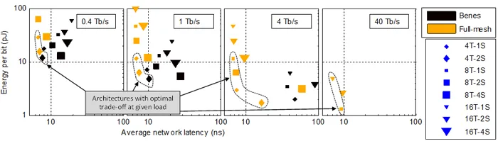
Check out our recent Hot Interconnect paper which compares various Chip-to-Chip silicon photonics based interconnection architectures in terms of realized bandwidth and energy-efficiency. According to our predictions, the critical metric of 1pJ/bit can be approached, in particular if inter-chip traffic is sustained at Tb/s rates.
This effort includes the analysis of the workload distribution over multiple node on the traffic intensities. We also analyze how interconnection networks with distinct capabilities affect distributed tasks. In this context, we proposed at the IA^3 workshop (part of SuperComputing'13 conference) a synthetic task model to ease such analyses.
Interaction with other simulation platforms
Acknowledging the major role played by data-movement in future systems performance, computing system simulators, as the Structural Simulation Toolkit (SST) effort of Sandia National Laboratories/DOE, are modeling interconnection networks with increasing fidelity. We are collaborating toward a seamless integration of optical-based data-movement capabilities in such simulators (along the lines of this position paper). This work is realized in the context of two Sandia/DOE funded research projects, Data-Movement Dominates and Co-Design and Optimization of Silicon Photonic Enabled Communication Architecture for High Performance Combustion Simulations.
Leveraging SST's full application simulation capabilities, we have been able to analyze the negative impact of the connection-oriented nature of optical communications on classical scientific application performance, and envisage network management policies able to mitigate this negative impact. Another ongoing research effort consists in identifying the optical interconnection network design leading to a minimized energy dissipation when executing a scientific workload. If scarcely dimensioned optical networks are less consuming, they also cause application slow-down which extends the whole system on-time. In contrast, ultra-wide networks show an important energy dissipation but lead to expedited application execution.
Toward Exascale computing thanks to photonic interconnection systems
An important effort of the modeling and simulation team consists in investigating how emerging technologies like silicon based nanophotonics may enable efficient Exascale computing, i.e. allow a super-computer to attain 10^18 operations per second. The extreme requirement of Exascale computing make optical transmission technologies potentially the sole enabling technology. This offer a unique chance for photonics to definitively penetrate in the computer architecture.
This research effort led to an estimation of the switch radix required to realize an Exascale computer. We also recently compiled an extensive review of major challenges associated with introducing Silicon Photonics in Exascale systems.
The miniaturization of switching elements and large-scale integration of nanophotonics gives rise to a critical challenge to the internal processing of the optical data packets while maintaining a memory-free switching fabric. We have developed a new routing approach specifically designed to accommodate the unique nano-scale integrated optical interconnection network, called SPINet (Scalable Photonic Integrated Network). SPINet is a novel optical packet switching architecture that does not employ optical buffering of any kind within its switching nodes; consequently, messages are dropped upon contention. A novel physical layer acknowledgement protocol allows for a dropped-message detection mechanism in which an optical acknowledgement (ack) pulse is sent from the receiving port upon successful transmission. SPINet leverages broadband WDM to offer high transmission bandwidths through a wavelength-striped packet format.
A 4×4 experimental network test-bed has been implemented with complex programmable logic devices (CPLDs) and discrete components, demonstrating critical network concepts such as address encoding and decoding, correct routing and switching, and error-free transmission of high bandwidth messages in the presence of ack pulses.
The SPINet network test-bed is comprised of 2×2 SOA-based photonic switching nodes, offering wideband transmission, data transparency, and packet-rate granularity. An experimental prototype switching node verifies its performance, demonstrating an average bandwidth exceeding 40 Gb/s per port and error-free routing of 160 Gb/s peak bandwidth.
Within the scope of the SPINet network simulations and test-bed, we have introduced the concept of path diversity as a means of increasing the utilization of optical packet switched networks. The network test-bed also demonstrates a high level of flexibility and programmability, straightforwardly supporting both synchronous and asynchronous traffic as well as priority-encoded optical packets. The interoperability between the optical network test-bed and an interface buffer has demonstrated dynamic queue management and cross-layer signal communication. The SPINet OPS network test-bed has also been adapted to support a programmable high bandwidth multicasting operation with mixed data rate packets [Lai OFC 2009].
The silicon material system endows novel optical devices with exceptional performance for diverse applications ranging from short-haul optical communication links to on-chip interconnection networks. Its complementary metal-oxide-semiconductor (CMOS)-process compatibility enables low-cost, high-yield fabrication of monolithically integrated circuits that can combine the best of optical and electrical functionalities.
The large index contrast in silicon photonic devices enables waveguides with low bending losses and engineered dispersions, empowering a broad and flexible design space complemented with immense dispersion tunability. Leveraging this tuning capability, silicon waveguides have recently become a promising platform for ultrafast all-optical parametric processing based on four-wave mixing (FWM), supporting future transparent optical networks with data rates approaching 1 Tb/s per wavelength channel.
We have demonstrated ultra-broadband wavelength conversion in these silicon photonic waveguides at the data rates of 10 and 40 Gb/s. Using critical quantitative system-level performance metrics, we quantitatively characterized these devices. In order to further demonstrate data rate transparency and scalability of this method, we have subsequently demonstrated all-optical wavelength conversion approaching hundreds of gigabits-per-second.
Broadcasting and multicasting of optical messages, critical network processes associated with the selective dispersing of information across many nodes, have traditionally been performed in the electronic domain using power-hungry optical-electronic-optical (O-E-O) conversion�as the data rate increases, the energy consumed by the serializers and deserializers alone quickly becomes the energy dissipation bottleneck in these systems. We have presented for the first time the use of FWM for all-optical wavelength multicasting on-chip in the silicon platform using the same dispersion-engineered silicon photonic waveguides. The all-optical processes using this inherently optically-transparent method are scalable both in multicast number and data rate.

Keren Bergman, Columbia University
David Keezer, Scott Wills, Georgia Institute of Technology
Please click here and here to download the videos embedded in the presentation.
Keren Bergman, Columbia University
Gary Carter, University of Maryland Baltimore County
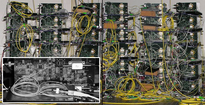
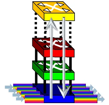
This project aims to develop a scalable architecture for an optical packet-switching (OPS) fabric for use in massively parallel high-performance computing systems. The goal is to provide large-bandwidth, low-latency connectivity between each of the users (e.g. processing nodes and memory banks) in such a system. The data vortex is a distributed deflection-routing interconnection network architecture designed to fully exploit the properties of fiber-optic technology in order to achieve ultrahigh bandwidth, low latency, and a high degree of port-count scalability. Utilizing photonic switching elements which facilitate transparent, broadband, self-routed optical packets, we have constructed a complete 36-node 12×12 optical switch with terabit-per-second scale routing capacity (see images below). This is the first complete implementation of a truly OPS network where no central arbitration is required. The system is capable of routing packets with immense bandwidths—160 Gb/s (10 Gb/s per channel × 16 wavelength channels) has been demonstrated but much higher rates are possible—from any one of the 12 input ports to any one of the 12 output ports, providing a median (and average) latency of 110 ns.
A number of experimental investigations of the system behavior have been performed, demonstrating for instance the flexibility of the system to power and timing variations. Additionally, injecting packets with varying duration and varying numbers of wavelength channels into the network simultaneously has verified the system’s robustness to variable message sizes.
Although the implemented switch fabric accommodates 12 ports, the intended application requires extensive scalability to harbor multi-thousands of users. The precise photonic implementation of the physical layer in such scaled systems may limit the physical size and usable bandwidth. Because SOAs are employed as the key switching element, understanding their performance characteristics is important to optimizing the system. A recirculating testbed environment has been implemented to experimentally study the physical limitations of OPS networks induced by the individual switching elements. This testbed has enabled unique physical layer analysis in the context of system scalability investigations, the effects of different modulation formats, and the first investigation of polarization dependent gain in OPS networks. Modeling and simulation of the physical-layer behavior are used in conjunction with the experiments to optimize the information carrying capacity and efficiency in future OPS network implementations.
For a full overview of our body of work related to the data vortex OPS interconnection network systems and subsystems, as well as many improvements that we have made to the original fabric, see our recent invited paper in the Journal of Lightwave Technology.
To address the need for a practical solution for buffering optical packets, we have developed a novel optical packet buffer architecture. The transparent buffering design is comprised of identical SOA-based building-block modules, yielding straightforward scalability and extensibility. In a time-slotted manner, the buffer supports independent read and write processes without packet rejection or misordering. Both first-in first-out (FIFO or queue) and last-in first-out (LIFO or stack) prioritization schemes have been experimentally realized. Further, active queue management (AQM) can be implemented on the buffer architecture to allow for network congestion control. Simulations have verified the improved buffer performance with latency, and experiments have demonstrated the functional verification of the optical packet buffer modeling AQM. The basic optical packet buffer architecture has also been adapted to realize network interface packet injection control for an optical packet-switched network, accepting backpressure and controlling the traffic injected into the network.
Global Environment for Network Innovations (GENI) is a NSF research agenda for clean-slate Internet design, experimentation, and collaboration to support experimental research in network science and engineering. The scope of our GENI project Embedded Real-Time Measurements (ERM) specifically ensures that the future GENI network infrastructure includes the appropriate technology to support cross-layer communications. By collaborating with other control frameworks, we endeavor to realize the ability within GENI to incorporate a diverse set of real-time measurements in networking protocols. The project addresses the GENI challenge of architectural experimentations across diverse heterogeneous technologies by supporting real-time cross-layer communications and measurements. Our objective is to develop networking capabilities within the future GENI infrastructure that enable deeper exposure of cross-layer information and user access to real-time measurements.
Within this project, we have developed a set of GENI requirements for real-time measurements and defined specifications for GENI networking protocols, recommending the use of an integrated, unified measurement framework. In addition, our project involves performing discrete-event simulations of cross-layer based networks in ns-2 and OPNET. Current work involves the experimental verification of these concepts.
This work continues along similar lines of the previous sections covering SPINet and POPS with the focus of using integrated optical systems to provide connectivity between many users. Here, though, the users envisioned are board-level elements that would be found in a typical computer system, such as processors, memory banks, or I/O devices. The goal of the project is to develop an integrated photonic switching system that delivers high-bandwidths to a large number of these users, and can be switched at sufficiently high speeds (nanosecond-scale) to facilitate message exchange in a very dynamic system where communication patterns are constantly changing.
Utilizing the functionality of many of the silicon photonic components explored through other research by our group, a wide variety of complex switching systems can be envisioned, which can each be integrated on a single chip providing connectivity to the local computational elements. Due to the large design space for such a system, it is important to compare both network and physical layer performances among the many alternatives. Therefore, we have developed a simulation environment which can monitor network performance (e.g. latency and throughput) for varying traffic patterns and user configurations, while also aggregating the physical-layer metrics (e.g. insertion loss, crosstalk, and power consumption) of the system in order to obtain the full view of how the system behaves. Such a simulation environment provides (1) a pre-fabrication performance comparison between competing designs, (2) perspective on how physical device improvements enhance system performance or similarly what device performance is required in order to achieve the desired level of system performance, and (3) an abstraction (similar to electronic CAD tools) of rigorous physical-layer modeling algorithms, which enables the investigations of more complex systems.
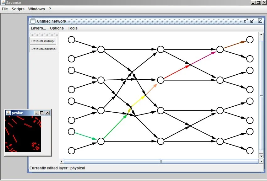
The image above represents a snapshot of the video to the left. In the image, a number of the 1×2 switches, 2×2 switches, waveguide crossings, and bends are arranged in the simulator to form the 4×4 non-blocking photonic router. The video depicts a brief demonstration of the simulator, which was implemented on the OMNeT++ platform. We develop the photonic device models in a hierarchical manner that allows us to describe in high detail several basic building blocks, and from these to construct larger functional components and even entire large-scale topologies. The animation begins by demonstrating the message transmission protocol on a photonic torus network. The left window shows the photonic plane and the right window shows the electronic control plane. We first see a message being transmitted along an electronic path which constitutes a path-setup, and subsequently data transmission occurs on the photonic plane. Near 45 seconds into the animation, the multi-level design methodology that our simulator leverages is illustrated when a user opens a single tile in the photonic network. Next, one of the 4×4 switches found within the tile is opened, and finally the viewer gets to peer into one of the basic building blocks that is explicitly programmed within the simulation. It is at this level that the physical device parameters may be altered.
The Future of Microprocessors
Recent developments in the microprocessor industry have indicated the end of the uniprocessor design and the emergence of multi-processor architectures. Chip designers have reached the limit of instruction-level parallelism that can be exploited with better pipeline design, as well as the improvements from clock scaling due to packaging and technology constraints. However, the emerging class of multi-processor systems raises a new problem in the interconnection network, the medium that allows all the processors, memory, and IO devices to communicate.
Typical modern day on-chip interconnection networks are implemented as electronic packet switched topologies. In some multi-core architectures, the network accounts for over 50% of the total power consumption of the chip. This proportion will be exacerbated as workload demand on these on-chip networks increases. Also, off-chip bandwidth is limited to the number of metal wires that can be traced off the limited peripheral area, which results in a large mismatch in on- and off-chip bandwidth. In order to alleviate these issues of power and bandwidth, one proposed solution that we and the research community are actively pursuing is the use of a photonic interconnection network.
Bringing photonics to the chip-level can potentially bring increased bandwidth, reduced latency, and improved power efficiency. The main advantage of on-chip nanophotonics lies in the decoupling of distance with power consumption. For chip-scale distances, signals can be modulated once and carried completely to their destination regardless of how far away it is. Conversely, electronics requires buffering every few millimeters, which consumes more power as data travels further. In addition to this key advantage for on-chip communications, photonics brings the added advantage that this concept also applies for chip IO, while maintaining the same bandwidth delivered on-chip! Speed of light in silicon end-to-end propagation can also yield significant improvements in latency. Because optics is not constrained to the common electrical restrictions that prevent high signaling rates across interfaces, it effectively solves the bandwidth mismatch.
Comprehensive Photonic Network Simulator
We are currently developing Photonic and Electronic Network Integration and Execution Simulator (PhoenixSim), a cycle accurate photonic interconnection network simulator suite on top of the OMNeT++ environment. The package is primarily composed of four simulation planes: the photonic plane, the electronic plane, the processing plane, and the IO plane. The photonic plane is a hierarchical structure with very detailed physical models of a number of photonic building blocks which can be used to create more complicated photonic structures, such as a switch or a network. The electronic plane acts as both a way to control the photonic network as well as an independent conventional electronic network, which typically shadows the photonic layout. The processing plane contains the modules that generate traffic, whether it be random, trace-based, or from cycle accurate instruction execution. The IO plane contains DRAM and other storage modeling, as well as bridges to other systems.
This simulation environment is being developed in an extremely dynamic and customizable way to enable it to be used in a variety of ways. The suite can analyze photonic networks at both the physical level, looking at parameters such as insertion loss and crosstalk, as well as at the system level in order to examine network and application performance. This functional diversity is enabled by the variety of other powerful open-source modeling packages we incorporate to increase accuracy. This includes, among others, the cycle accurate micro-architectural simulator SESC, the electronic router power model package ORION, and the DRAM functional and power model DRAMsim.
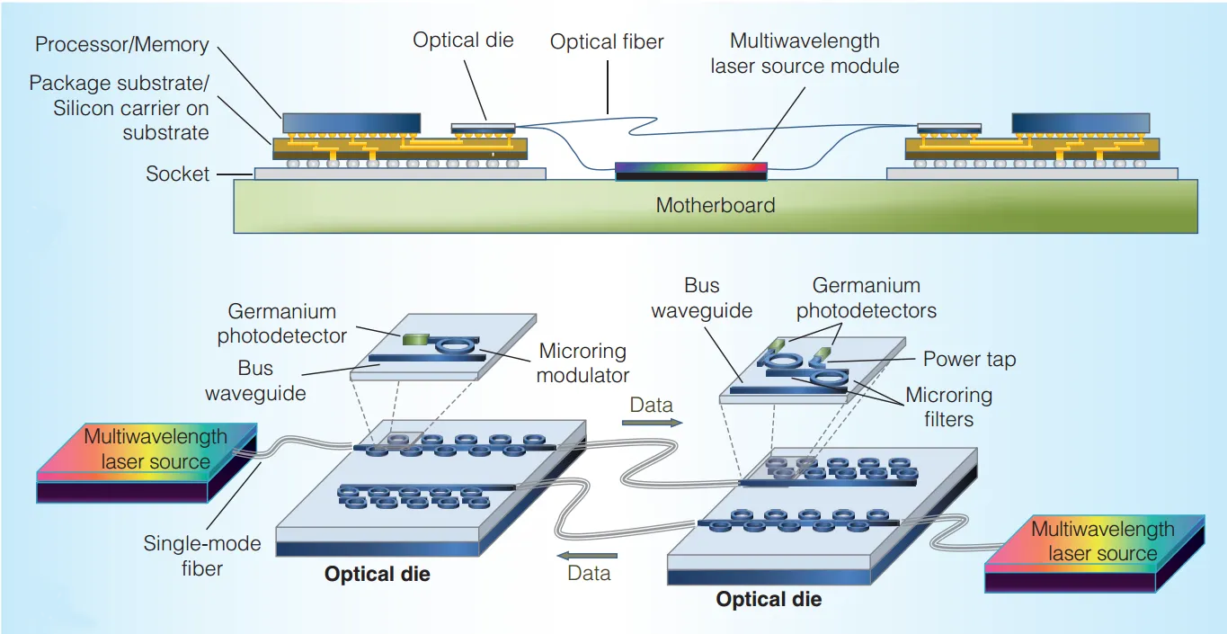
Photonics for Board-Level Communications
Currently we are investigating ways to bring photonics to both the microprocessor chip and the motherboard. Current computing systems suffer from a bandwidth bottleneck between the processor and memory. Typically processor designs use caching to help hide the latency, but as the number of cores on chip grows, as will the network complexity, careful deliberation of the communication architecture will be extremely important.
Nanophotonic CAD Environment
We are also developing Visual Automated Nanophotonic Design And Layout (VANDAL), a CAD environment for nanophotonic interconnects.
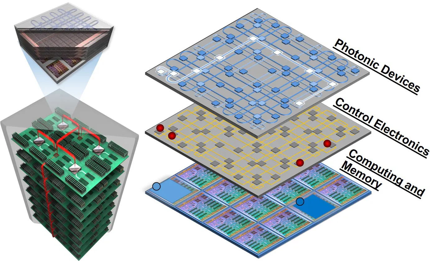
Recent advances in silicon photonic micro-fabrication techniques—the same highly-developed techniques used in the commercial development of the ubiquitous complementary metal–oxide–semiconductor (CMOS) platform—have led to the expansion of a photonic toolbox consisting of key elements which enable the realization of chip-scale photonic interconnection networks in the context of networks-on-chip (NoCs) interconnecting chip multi-processors. Collaborating with leading research groups in this area, we have developed a network-driven design approach for implementing and characterizing these building blocks. Our vision includes a three-dimensional integrated (3DI) monolithically-integrated silicon stack, comprising traditional CMOS and dynamic random access memory (DRAM) technology as well as optoelectronic and other photonic integrated circuit (PIC) devices. Among the components that we have investigated to support our vision is an electro-optic form-factor translator, which converts space-parallel data from an electronic bus into wavelength-parallel photonic data coinciding on a single waveguide link. We then investigated the ultra-broadband, low-loss photonic link capable of carrying terabits-per-second of information encoded in this wavelength-parallel manner from one node to another.
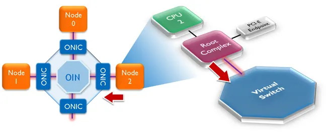
Providing a seamless gateway from the compute nodes to the photonic network represents a key enabler for the realization of an end-to-end optical interconnection fabric. Format and data rate mismatches at the electronic/photonic edge necessitate the development of a unique network interface to address these critical bottlenecks. The design and development of an Optical Network Interface Card (ONIC) that will address these challenges to latency and bandwidth scalability is currently underway.
The ONIC manages the encoding, packetization, and multiplexing/demultiplexing of serial electronic data to a wavelength-parallel optical format in a low-latency manner that is transparent to the interconnected compute nodes. By abstracting away the interconnection network, the attached compute nodes can exploit the capacity of WDM – supporting high-bandwidth multi-wavelength striped message exchange – while being completely agnostic to the details of the underlying photonic interconnect.
The advancement of various standard protocols, such as PCI Express and InfiniBand, has enabled interconnectivity among diverse communicating modules and processors. By leveraging field programmable gate array (FPGA) technology, we have flexibility in the definition of the data exchange protocol, optical message structure, timing, and synchronization. This flexibility thus allows for the architectural exploration, experimental testing, and design validation of a variety of computing systems supporting different communications protocols.
PCI Express
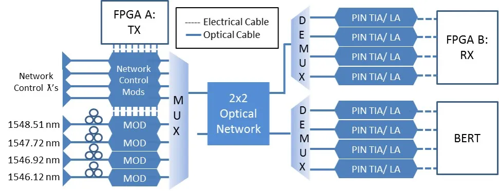
PCI Express (PCIe) has emerged as the preeminent protocol standard for high-bandwidth chip-to-chip communication in current and future generation computing systems. PCIe is based on packetized serial point-to-point links and, in its current iteration, can support up to 16 data lanes per link signaling at 8 Gb/s per lane.
We have developed an all-optical photonic interface capable of transparently formatting serial data streams, such as PCIe, into high-bandwidth wavelength parallel photonic packets. Employing the aforementioned photonic interface, we have also demonstrated the end-to-end generation of a PCIe link originating from a remote endpoint across the interface to a host computer. The remote endpoint is implemented on a customized FPGA-based device. PCIe traffic originating from the endpoint and logically routed through the established PCIe link is demonstrated via direct memory accesses (DMA) initiated by an application running on an x86-based PC. Successful transmission of PCIe data at 2.5 Gb/s and maintenance of the logical PCIe link was experimentally confirmed across eight wavelengths.
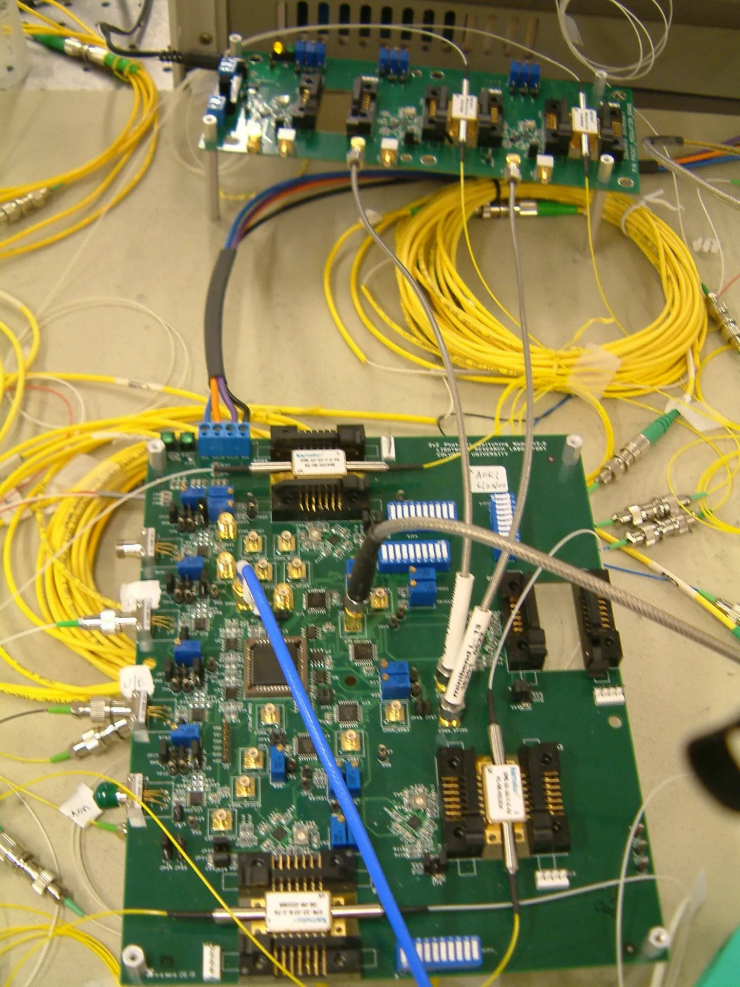
InifiniBand
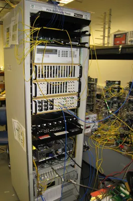
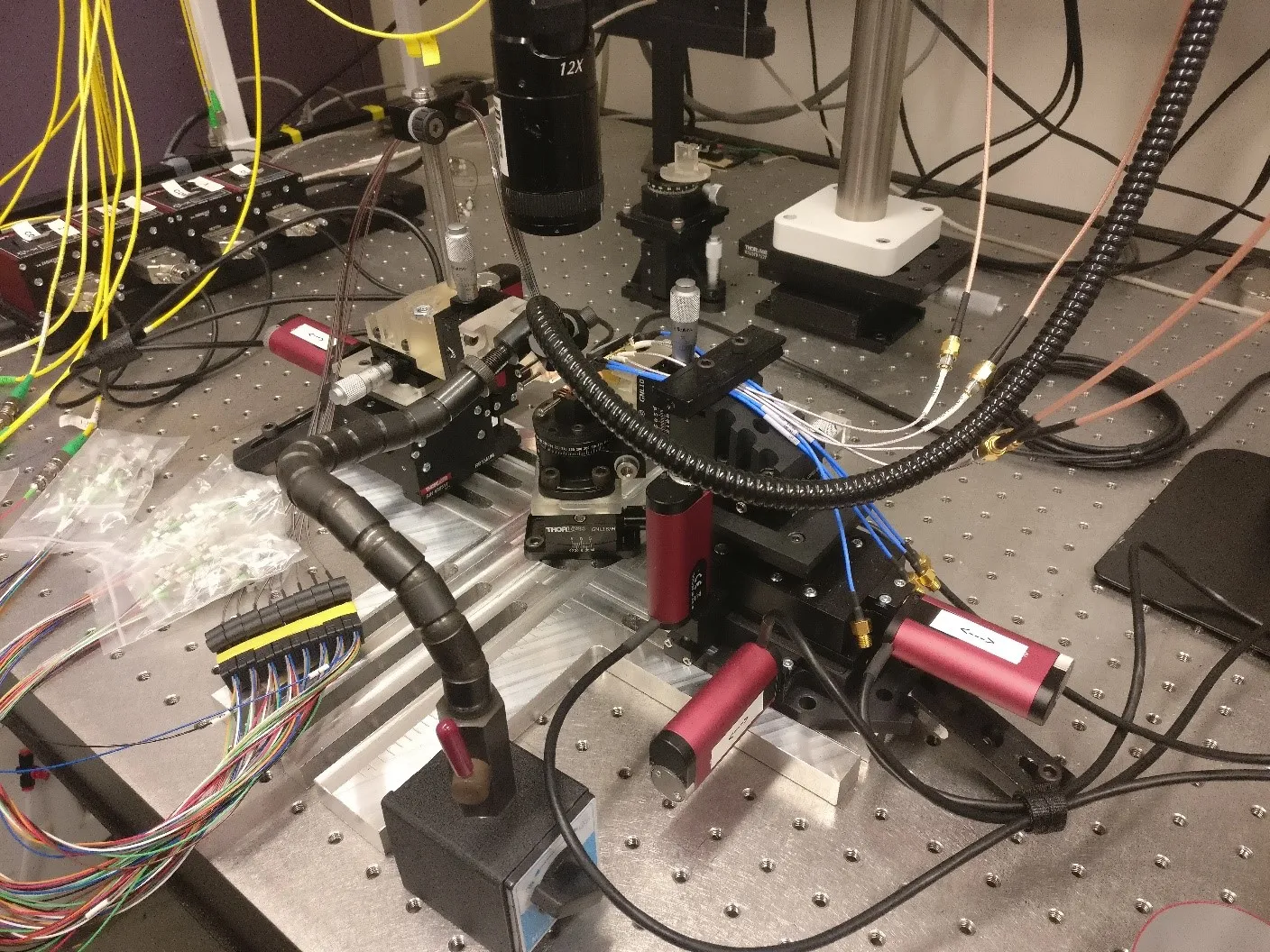
InfiniBand is a switched-fabric interconnection network prevalent in today's high-performance computing systems. Infiniband routes variable-sized packets from source to destination at high data rates and low latencies. And like 10 Gigabit Ethernet, the individual copper cables linking the network together have been replaced with WDM fiber optics. However, the Infiniband switches are still electronic, necessitating an optic to electronic conversion at every switch in the network. Our research aim in this arena is to transparently send Infiniband packets over our optical packet-switched networks. To achieve this goal, we are adapting an off-the-shelf FPGA board to decode the Infiniband packet from a standard Infiniband HCA (essentially a network interface card) and transport it out over our optical network. The picture at left shows some of our test equipment, notably the FPGA board and physical adapters. We are working to expand our test setup to create a point-to-point link between two Infiniband HCAs using our optical packet format.
Interconnect Fabric System Test-Bed
In order to evaluate critical architectural design considerations a macro-scale test-bed environment consisting of high-performance blade-level CMP compute nodes interfaced to an optical interconnection network via the aforementioned ONIC is currently under development. This interdisciplinary effort will leverage ongoing research in optical interconnection networks, low-latency photonic network interfaces, and communication intensive applications to create a coherent end-to-end prototyping environment. The implemented test-bed will facilitate the experimental validation of end-to-end optical message exchange in various hardware platforms and topological configurations, enabling realistic investigation of critical architectural concepts and real-world performance characterizations. Specifically, the test-bed will provide a platform for investigation of optical address encoding/decoding methods, demonstration of photonic end-to-end payload routing and transmission, and evaluation of interface/routing latencies and throughput scaling in a practical environment. Furthermore, by executing realistic application driven traffic on high-bandwidth inter-node optical communications platforms, this demonstrator will provide a means for evaluating high-performance WDM infrastructures as full network solutions for CMP-based advanced computing systems. It is our vision that the successful implementation this interconnect fabric system test-bed will help bridge the gap toward practical use of optical interconnects in future high-performance computing systems.
In an effort to bridge the gap between academic research and real-world application, we are collaborating closely with the engineers at Intel Research towards a path for viable commercialization of optical interconnects supporting multi-wavelength striped message exchange for high performance cluster computing. The focus of our collaboration includes the design and development of a unified experimental platform consisting of the ONIC and the interconnect fabric system test-bed. Investigations on various real-world performance metrics and design considerations will be conducted with continual interactions with Intel engineers to enable a cohesive partnership exploiting the resources and expertise of each group.
It is becoming increasingly clear that a clean-slate architectural design of the network protocol stack is an essential target for next-generation IP networks and network routing applications. A major challenge in realizing the required enhanced capabilities in next-generation networks lies in overcoming the current limitations due to the rigid notion of network layering. To address the research agenda of future networking infrastructures, our goal is to achieve a cross-layer communication infrastructure to provide bidirectional information exchange between layers. Enabling programmable interaction with the optical substrate will allow the higher layers dynamic access to the full optical bandwidth. Our goal is to create an intelligent, dynamic, programmable, network and application layer aware optical substrate, where data introspection and optical performance monitoring measurement data can be leveraged for cross-layer communications to impact network routing and performance.
The AIM Datacom project is a joint effort between our group and researchers at UCSB that aims at driving low cost and energy efficient designs that enable next generation data center network architectures.
 Modular switch architecture b) 3D integration including electrical PCB and optical interposer, (c, d) Top and side view of high-radix switch architecture with amplifiers between stages.")
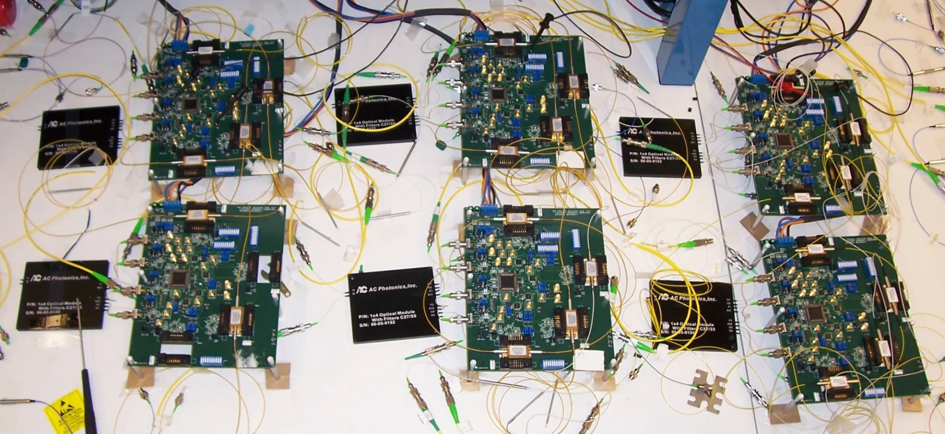
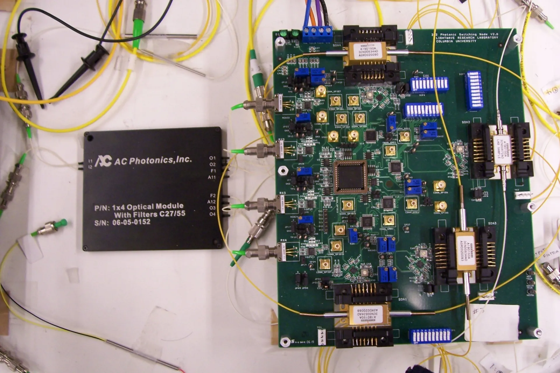
The AIM Test Project seeks to develop cutting-edge testing solutions for the field of silicon photonics. The focus is the implementation of an automated, switch-centered testing approach for chip, wafer and package-level photonic devices. To this end, the Testing team at the Lightwave Research Laboratory has constructed software framework for controlling automated functional test tools (Prober Control), designed and verified a new approach for wafer-scale optical probing, and developed innovative photonic component measurement strategies.
Lightwave Research Lab has driven functional testing efforts for the TAP Hub since 2016. Columbia’s main responsibilities include providing technical support during the equipment procurement process, and the development of the complete automated functional test platform design for implementation, control, and user access at the TAP Hub. We have further trained TAP Hub engineers on the platform. The switch centered
architecture consists of a rack of test and measurement equipment interconnected via RF or optical switch and automated control plane software to the prober system.
Photonic integrated circuits (“PICs”) are projected to scale into dense circuits with hundreds or thousands of elements in the near future. Automated testing of these increasingly complex PICs is a key challenge for the functional testing efforts at the AIM Photonics TAP Hub. A critical aspect is the identification of known good die at the wafer scale. To accomplish this goal, we will work in partnership with Cisco to develop a set of test structures implemented within the dicing channels. The test set and automated electro-optic testing script pass-criteria will provide a platform for performing automated wafer scale functional testing to identify and map validated good dies.
The E2CDA project is a collaborative effort between Dr. Alex Gaeta (Applied Physics and Math), Dr. Michal Lipson (Electrical Engineering), Dr. Luca Carloni (Computer Science), and Dr. Keren Bergman to develop next generation application-specific optical computing systems. The student working on and leading the E2CDA project from LRL is Natalie Janosik.

With Moore’s Law slowing down, it is critical to explore alternative computing technologies to sustain the progress of chip-multiprocessor systems. We are developing photonic interconnection networks for chip-multiprocessor computing systems by capitalizing on the high parallel processing capabilities exhibited in SiP microarchitectures to accelerate target applications using electronic-optical co-design.
Ongoing applications include an opto-electronic and integrated Ising solver and Optical Matrix Multiplication Unit (OM2U) as seen in Fig. 2.
 Target application classes include deep learning and ising solvers where our photonic microarchitecture overlaps (left). (b) Opto-electronic co-designed accelerator for both neural networks and ising solvers (right).")

Free-space laser links used for satellite communications are currently limited in modulation speeds due to the high power-per-bit consumption of the optical transceivers. In this project we take advantage of recent breakthrough 3D monolithic integration of photonic structures, particularly high-speed graphene-silicon devices on CMOS electronics in order to create CMOS-compatible high-bandwidth transceivers for ultra-low power terabit-scale optical communications. The target signal integrity and end-to-end energy-per-bit are set as the figure of merits for the inter-satellite free-space link. The parameters subject to optimization in the design space are the modulator’s bandwidth, thermal control of optical devices, and the tradeoff between required net coding gain (NCG) and modulation overhead.
The graphene modulator’s operation bandwidth is not limited by the carrier transport in graphene, but it is bottlenecked by the parasitic components of the modulator circuit. These parasitics are the capacitor formed by the graphene-dielectric-graphene stack, graphene-sheet resistance, and graphene-metal contact resistance. While it is possible to design the device footprint in such a way to reduce the capacitance and the sheet resistance, and simultaneously optimize both modulator performance and operation bandwidth, the contact resistance is fundamentally related to how the metal-graphene interface is formed. Previously, surface contacts have been employed to interface the metal and the graphene, where the metal is deposited at the graphene’s top surface in order to form contacts. The metal and graphene interaction in the surface contacts approach occurs perpendicularly to the graphene molecular two-dimensional (2D) plane. Since graphene’s vertical orbital hybridization is weak, surface contacts are fundamentally incapable of maximizing metal and graphene interaction. In this project our team is aiming at exploring novel ways to break through this barrier and achieve ultra-high bandwidth graphene-based (and other 2D material-based) silicon modulators.
 WS2 (TMD) – HfO2- ITO parallel plate capacitor configuration designed to introduce charge carriers in the monolayer TMD material. (b) Schematic of a phase shifter design where the capacitor is placed in the middle of the waveguide with maximum mode overlap. (c) Device cross section showing WS2-HfO2-ITO capacitor on a Si3N4 waveguide. The inset indicates the position of WS2 in the mode-profile of the waveguide configuration. (d) Optical micrograph of the fabricated device. Dashed inset shows the location of the patterned WS2 on the left arm of the MZI (yellow).")
 Transmission response of the MZI for different voltages applied across the WS2 – HfO2 – ITO capacitor located on one of the arms of MZI. Extracted (b) change in effective index and (c) change in absorption measured from the MZI spectra in Fig. 2 (a) of the composite SiN – WS2 waveguide. (d) Frequency response (S21) of the phase modulator measured at 1550 nm. The device has a 3 dB bandwidth of 0.33 GHz. (e) Change in imaginary part of the optical sheet conductivity of monolayer WS2 with voltage, extracted from the change in effective index in Fig. 2 (b) by calculating the mode overlap using COMSOL simulations. The inflection point at -4 V in Fig. 2 (b), (c) and (e) illustrates the charge neutrality point for the monolayer WS2, indicating that the monolayer was initially n-doped with electron densities of 1.38 × 1012 cm-2 either during transfer or due to substrate effects.")
Columbia team works jointly with HPE’s PathForward program in an integrated multidisciplinary effort to leverage photonic, system architecture, and software expertise to develop new photonic enabled Exascale systems designs and drive emerging integrated photonic interconnect technologies. The leading researcher of the PathForward project from LRL is Yanir London.
Perhaps the most critical barrier toward realizing Exascale computing is the fundamental challenge of data movement. With the extraordinary growth in parallelism at all scales, even in today’s systems, performance is increasingly determined by how data is communicated among the numerous compute-memory resources rather than the total raw computation. Data movement challenges impact the entire system stack: from the physical architecture and memory hierarchy to the algorithms and software development that must manage the immense growth in parallelism. At Exascale, these challenges grow, as energy consumption can be dominated by costs of data movement and thereby imposes constraints on the ultimate performance.
The main challenge for interconnect technology has always been to provide sufficiently high network bandwidth and message rate, while maintaining as low a latency as possible. However, more important than the raw interconnect performance in these areas, is how effectively applications are able to utilize the network. Historically, many interconnects have been built to provide these capabilities without regard to the communication mechanisms being used by the applications running on the system, leading to a bad semantic match between the communication primitives required by the applications and those provided by the network.
High performance interconnection networks that are intimately co-designed with the hardware and software and take advantage of the transformational advantages of photonics will directly impact the execution performance and scalability of Exascale DOE applications. Photonic technologies represent the most promising path toward realizing a fundamentally energy efficient system interconnect that can scale to meet Exascale bandwidth requirements. The Columbia team works jointly with HPE’s PathForward program in an integrated multidisciplinary effort to leverage photonic, system architecture, and software expertise to develop new photonic enabled Exascale systems designs and drive emerging integrated photonic interconnect technologies.